Journal of Machine Intelligence and Data Science (JMIDS)

Volume 5 - Year 2024 - Pages 94-108
DOI: 10.11159/jmids.2024.011
Next-Gen Computational Modeling for Transformative Electroforming Processes
Ilhem Boutana1, Oussama Boultif2, Abdessalam Zait2
1Laboratory of Electrical Engineering and Industrial Electronics, Faculty of Science and Technology
University of Jijel, 18000 Jijel, Algeria
hafsaoui@univ-jijel.dz
2Electrical Engineering Department, University of Jijel
Jijel, Algeria
boultifoussama3@gmail.com; abdessalamzait@gmail.com
Abstract - Electroforming is an advanced manufacturing process that uses electrolysis to deposit metal onto a substrate, allowing for the creation of highly intricate and detailed metal components. This technique is widely utilized in industries such as jewelry, electronics, and art, where precision and complexity are critical. Additionally, electroforming is essential in producing molds, prototypes, and high-precision parts for applications in the aerospace and automotive sectors. The process excels in generating complex geometries with exceptional accuracy. Modeling electroforming involves simulating the physical and chemical interactions during metal deposition to optimize parameters, predict performance, and improve the quality of the final product. Although modeling is complex, it plays a crucial role in enhancing the efficiency, precision, and cost-effectiveness of the manufacturing process. By simulating these factors, manufacturers can refine their methods to reliably produce high-quality electroformed components. In this study, a 2D, time-dependent, secondary current distribution model, developed in COMSOL Multiphysics, is employed to validate the electroforming of copper and nickel devices across various processes, providing valuable insights into process optimization and outcome prediction.
Keywords: Electroforming, Electrodeposition, Electroplating, Electropolishing, Numerical Modeling.
© Copyright 2024 Authors - This is an Open Access article published under the Creative Commons Attribution License terms. Unrestricted use, distribution, and reproduction in any medium are permitted, provided the original work is properly cited.
Date Received:2024-01-07
Date Revised: 2024-09-22
Date Accepted: 2024-10-02
Date Published: 2024-10-15
1. Introduction
Nowadays, Electrochemical forming, or Electroforming, is increasingly recognized as a sustainable additive manufacturing process that employs electrochemistry to build structures layer by layer [1]-[3]. Currently, many complex components for applications such as printing, holography, and sound reproduction are produced using electroforming. Additionally, several custom components in the aerospace industry rely on nickel and its alloys formed through electrochemical processes. Despite the continued use of electroforming in manufacturing, academic and scientific interest in the field remains limited, which is now hindering the transition to automated production (e.g., [4],[5]).
Electroforming, is a fabrication process for components through electrodeposition, with a fundamentally straightforward mechanism. The required metal is deposited onto a die submerged in a suitable electrolyte until it reaches a thickness sufficient for the structure to be self-supporting. The removal of the die effectively completes the production of the electroform. The die is shaped and finished to the required specifications, and while there may be minimal adhesion between the deposited metal and the die, the surface contour and finish of the die are precisely replicated on the contact surface of the electroform.
The interest in simulating the electroforming process is not a recent development. The first numerical studies of the process emerged in the 1970s. Since then, electroforming has been studied only sporadically, despite the rapid advancements in computer science. However, interest in the process, its applications, and its potential for more rigorous modeling has significantly increased over the past decade (e.g., [6]-[12]). Electroforming, in particular, involves changes in the shape of the reaction surface, and modeling these changes can be challenging. Meanwhile, experimental studies of this process have been conducted more systematically, providing data that facilitate the development of modeling tools. This underscores the importance of numerical modeling for electroforming, which allows for the simulation of various experimental operations in this technology—a key objective of our work.
Following these considerations, our paper consists of numerically modeling the shaping of industrial components, particularly surface treatment, using the electroforming process. Moreover, this paper is an extension of our short conference paper [13], where we presented our Electroforming-based approach for printed circuit boards (PCB) manufacturing using the Electrodeposition process. Indeed, this research significantly overcomes the contribution of the short paper by providing the following contributions:
- Numerical Modeling of Electroforming Process: developing a 2D time-dependent secondary current distribution model in COMSOL Multiphysics to simulate the electroforming of copper or nickel. This model helps to predict performance and optimize key parameters for better results.
- Enhanced Process Understanding: improving understanding of electroforming’s physical and chemical interactions, providing insights for optimizing the process to ensure high-quality outcomes.
- Validation and Assessment: offering comprehensive numerical evaluations for different applications, including electroforming, electroplating, and electropolishing, and providing theoretically validated results.
- Potential for Industry Applications: contributing to various industrial applications, including printed circuit board manufacturing, aerospace, and automotive industries, with potential improvements in manufacturing efficiency and precision.
- Electrodeposition and Electroplating Analysis: Investigating the effects of different materials (copper and nickel) and parameters (e.g., potential, current) on electrodeposition and electroplating processes.
The remaining parts of this paper are organized as follows. In Section 2, we provide an overview of state-of-the-art Electroforming process proposals. Section 3 focuses on providing an overview of numerical modeling of Electroforming processes along with the mathematical models. After that, Section 4 presents our comprehensive numerical evaluation and assessment for different applications. In Section 5, we present conclusions and possible future work.
2. Related Work
In this Section, we provide a comprehensive overview of state-of-the-art Electroforming process proposals.
In [14], the authors advance the understanding of nickel electroforming by scaling up from lab-scale experiments to industrial applications, specifically focusing on the electroforming of a mechanical vane—a critical component in the aerospace industry. By utilizing a 3D secondary current distribution model developed in COMSOL Multiphysics, they successfully simulate the electroforming process, achieving results that align with experimental findings conducted in an industrial pilot tank. The study demonstrates the model's ability to predict thickness distribution under various current densities and highlights its application for both quantitative and qualitative studies depending on operational conditions. Furthermore, the investigation into the electroformed surface characteristics, supported by scanning electron microscopy, provides insights into the microstructure and growth mechanisms of the nickel deposits.
[15] presents a sustainable method for recovering high-purity copper from waste printed circuit boards (WPCBs). By introducing ethanol as a dispersant in the flotation process, the authors significantly improve the efficiency of copper extraction from the WPCBs. Subsequently, electrodeposition is used to recover pure copper from the concentrated material. The study optimizes key parameters like solid-to-liquid ratio and applied voltage to achieve a high copper deposition rate while maintaining deposit purity. This work contributes to both resource recovery and environmental sustainability by providing an effective and environmentally friendly approach to recycling WPCBs.
[16] explores the use of pulse-reverse electrodeposition to fabricate Nickel (Ni) coatings reinforced with different carbon allotropes, including Carbon Nanotubes (CNT), Graphite (Gt), and Graphene (Gr). The authors investigate the impact of these carbon inclusions on the microstructural and electrochemical properties of the coatings. Various characterization techniques, such as Field-Emission Scanning Electron Microscopy, Atomic Force Microscopy, X-ray diffraction, and Raman spectroscopy, reveal that the addition of carbon allotropes enhances the structural uniformity and reduces surface roughness, with Ni-Gr showing the lowest roughness. Electrochemical studies using Electrochemical Impedance Spectroscopy and polarization tests demonstrate significant improvements in corrosion resistance, with Ni-Gr coatings achieving up to 60% better protection compared to pure Ni coatings. The reduction in corrosion current density further confirms the superior protective performance of the Ni-Gr composite coating.
In [17], they focus on the development of a black chromate conversion coating (CCC) for aerospace electrical connectors, aimed at achieving high corrosion resistance and excellent conductivity. The authors successfully electrodeposited a Zn-Ni alloy on 2024 aluminum alloy, followed by Cu+-based coloring to produce a uniform black conversion coating. The conversion solution was optimized with specific concentrations of CrO3, NaCl, CuCl, and HNO3. The performance of the CCC was evaluated using techniques such as electrochemical impedance spectroscopy (EIS), polarization curves, and conductivity testing. The results demonstrated that the coating improved the impedance of the Zn-Ni alloy, significantly reducing corrosion current density to thereby enhancing corrosion resistance. Additionally, the CCC exhibited excellent electrical conductivity with a resistance of only in a cylindrical connector specimen.
[18] investigates the effects of electropolishing on the surface characteristics and corrosion behavior of AISI 316L stainless steel specimens. The research evaluates various electropolishing parameters, including voltage, temperature, time, and cathode materials and geometry, using sulfuric acid, phosphoric acid, and water electrolytes. The surface characteristics were analyzed through scanning electron microscopy, X-ray diffraction, micro indentation tests, and contact profilometry, while corrosion resistance was assessed in a 3.5% NaCl aqueous solution. The findings reveal that electropolishing significantly reduces surface roughness when optimal parameters are applied, although waviness remains irregular. The use of stainless steel cathodes instead of copper improves surface smoothness. Electropolishing also removes the deformed surface layer and martensite phase, leading to a decrease in surface hardness but an enhancement in corrosion resistance. Additionally, cylindrical specimens achieved more uniform roughness when electropolished with a cylindrical concentric cathode compared to flat cathodes. This study enhances the understanding of how electropolishing parameters influence surface quality and corrosion resistance, providing insights for optimizing the process for stainless steel applications.
3. Numerical Modeling of Electroforming processes
In this Section, we present an overview of the numerical modeling of Electroforming processes along with the mathematical models used in our numerical evaluation.
Electroforming is a complex and widely utilized technique for fabricating microstructured components. Its nature is multiphysical, as it encompasses fluid dynamics, ion concentration, electric current distribution, and other interrelated physical phenomena. Therefore, modeling this process requires a deep understanding of the physical phenomena involved, along with expertise in mathematical modeling and a rigorous study with well-defined assumptions.
3. 1. Mathematical Models
The modeling of electroforming simulates the deposition process at PH=4, which implies that the proton concentration is very low compared to ion concentrations. For this reason, the material balance of protons does not need to be modeled. Deposition at the cathode and dissolution at the anode are assumed to occur with 100% current efficiency, meaning the model excludes any possible secondary reactions.
As a result, during the process, differences in electrolyte density arise within the closed cell, resulting in a higher density at the anode compared to the cathode. This can induces free convection within the cell. However, it can be neglected, as the variations in composition are minimal. Thereby, Equation (1) presents the Nernst-Planck Equation [19], which describes the movement of each ion in the electrolytes:

Where Ni is the transport vector, Di represents the diffusion coefficient, ci is the concentration of i ions in the electrolyte, zi is the charge for ionic species, ui is the mobility of loaded species i, ϕi the potential in the electrolyte, and F is the Faraday constant defined as F=96485,338 [C/mol].
Moreover, the material balances are expressed by Equation (2). However, for each species i=1.2, the criterion of electrical neutrality is stated by Equation (3):
and:

On the other hand, the boundary conditions at the anode and cathode are defined by the Butler-Volmer equation [20] presented in Equation (4).
Where ict is the local charge transfer current density, i0is the exchange current density, αa,mis the anode charge transfer coefficient, αc,m is the cathode charge transfer coefficient, R is the universal gas constant (i.e., 8.314 J/mol.K), T is the temperature at which the problem is studied, cm is the concentration of the metal in the solution, cm,ref is the reference concentration of the metal, and η is the activation overpotential, defined as follows:
Such that ϕs,0 is the electric potential of the respective electrode, ϕl is the potential in the electrolyte, and Δϕeq is the difference between the metal and electrolyte potentials.
3. 2. Electroplating Process
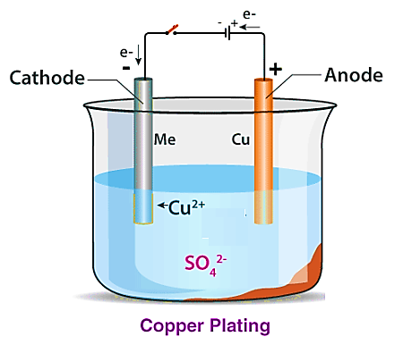
The electroplating process involves producing a metallic coating on a solid substrate by reducing metal cations using a continuous electric current. The part to be coated serves as the cathode of an electrolytic cell, the electrolyte is a solution of a metal salt, and the anode is typically either a block of the same metal or an inert conductive material. The current is supplied by an external power source. This model uses a secondary current distribution and applies full Butler-Volmer kinetics for both the anode and cathode. The anode dissolves while the cathode, often a part decorated with a finishing metal such as nickel, receives the deposited metal. Figure 1 shows a schematic view of the electroplating process.
In the case of electroplating, the electrodeposition model uses a secondary current distribution with full Butler-Volmer kinetics for metal deposition (such as nickel) or the dissolution reaction at the cathode and anode. A concurrent hydrogen evolution reaction is also present at the cathode. The thickness of the deposited layer on the cathode is calculated, along with the current efficiency. The overpotential for the electrode reaction at index m is defined by the following equation:

Where Eeq,m is the difference between the metal and electrolyte potentials at the surface of the electrode, measured at equilibrium using a common reference potential.

4. Results and Discussions
In this Section, we present our numerical evaluation and assessment conducted using the Electroforming process. Through this rigorous evaluation, we aim to demonstrate both the effectiveness and efficiency of our numerical models.
4. 1. Electrodeposition
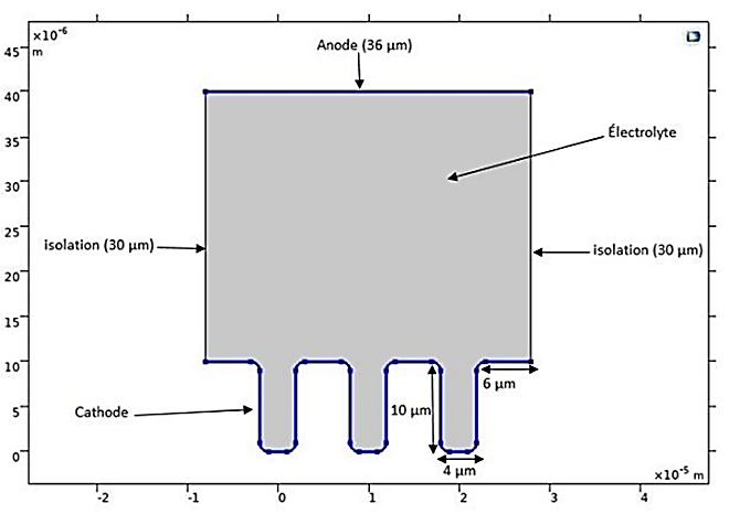
In this application, we aim to model the copper electrodeposition on a microstructure, specifically a printed circuit board with three small trenches or microcavities. The potentiostatic plating cell consists of an anode and a cathode. During deposition, the boundaries of the cathode and anode shift, making the simulation inherently time-dependent. Additionally, the copper deposition rate is not uniform across the cathode surface.
This application, which is based on a benchmark electrodeposition model, utilizes the “Electrodeposition” module of COMSOL software. The use of a deforming geometry allows for the analysis of the plating process and the study of the variation in the cathodic boundary during the electrodeposition process.
The geometric model of this application, shown in Figure 2, includes the anode and cathode, which form the horizontal boundaries of the cell containing the electrolyte. Potentials of ±0.1V are applied at the electrodes. In contrast, the vertical walls represent the pattern on the main electrode and are insulating.
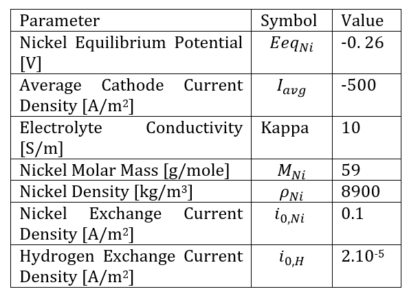
In this application of electrodeposition on a printed circuit board, and to study the effect of the material, we considered two commonly used materials in this process: copper and nickel. Therefore, two different electrolytes are used: CuSO₄ and NiOH. Table 1 summarizes all the parameters considered for the application and the boundary conditions used in both cases of copper and nickel electrodeposition.
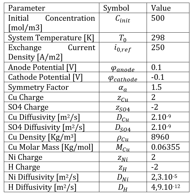
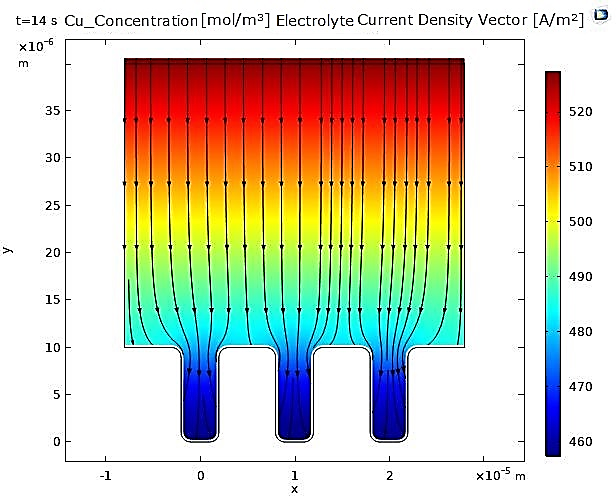
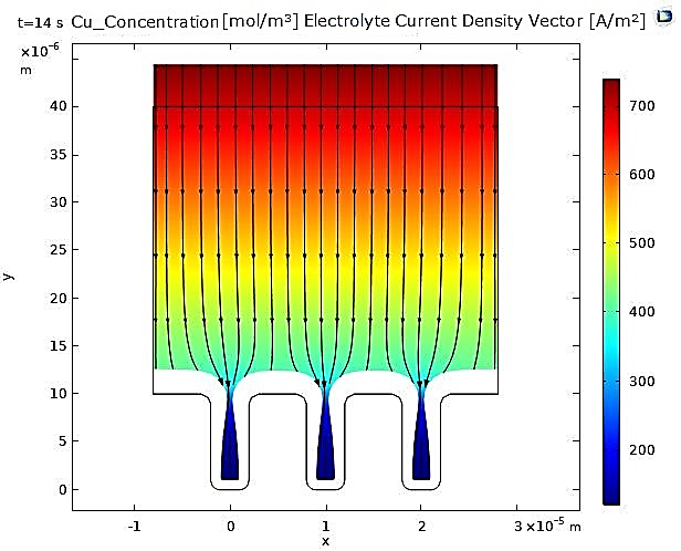
Regarding the current density vectors in the electrolyte, they are oriented from the anode to the cathode and show no significant difference between the copper and nickel cases. On the other hand, we can observe that the trench opening begins to narrow, caused by the increasing thickness of the deposit, which is non-uniform in the case of copper.
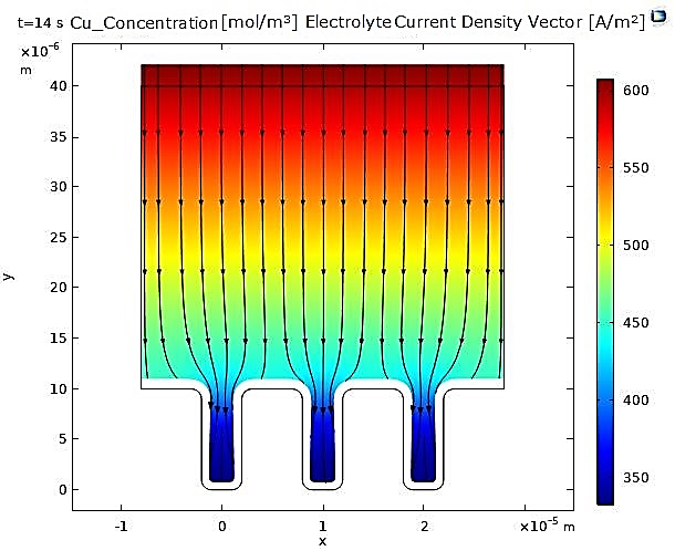
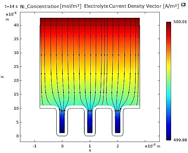
In contrast, for nickel, the narrowing of the microcavity is uniform due to the uniformity of the deposited nickel layer (see Figure 3 and Figure 4).
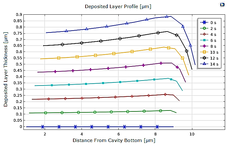
Figure 5 examines the thickness of the deposited copper layer along a vertical cathodic surface. This figure provides another way to observe the development of a non-uniform deposit. This occurs due to the uneven distribution of current density, which is further intensified by the depletion of copper ions along the depth of the cavity.
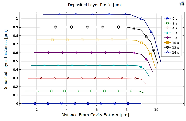
Moreover, it should be noted that by comparing the different profiles of the deposited layer at the cathode for copper and nickel, obtained from 0 to 14 seconds with a 2s interval, it is clear that in the case of nickel, the deposit is thicker but remains uniform, except at the edge of the cathode, as presented in Figure 6.
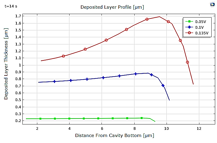
Additionally, we analyzed the effect of the applied potential at the electrodes on copper electrodeposition. The results show the significant impact of potential on the electrodeposition process. Indeed, the variations in copper ion concentration within the electrolyte are closely tied to the potential, and the copper layer deposited at t=14s is notably thicker at the higher potential of ϕ=0.135V (see Figure 8) and becomes negligible at the lower potential of ϕ=0.05V (see Figure 7).
Furthermore, the profiles of the copper layers deposited at the cathode for the three different potential values differ significantly. The thickness of the deposited layer and the non-uniformity of the deposit are notably accentuated at higher potentials as depicted in Figure 9.
In summary, the numerical results from this first application show that electrodeposition is highly dependent on both the nature of the deposited material and the applied potential. These results are theoretically predictable, as electrodeposition relies on electrochemical reactions, making the nature of the involved ions and the applied potential at the electrodes critical parameters.
4. 2. Electroplating
The second application concerns electroplating, a widely used technology for numerous technological applications, ranging from decorative coatings to high-precision passive electromagnetic shielding devices.
This electroplating model uses a secondary current distribution with full Butler-Volmer kinetics (see Equation (7)) for metal deposition or the dissolution reaction at the cathode and anode. A concurrent hydrogen evolution reaction is also present at the cathode. The thickness of the deposited layer at the cathode is calculated along with the current efficiency. Table 2 summarizes all the parameters for the electroplating applications.
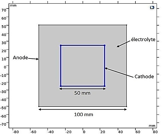
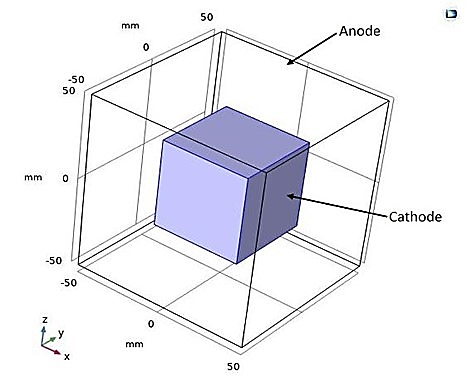
The 2D model geometry, illustrated in Figure 10, represents a microstructure component with small dimensions. The anode is a flat-dissolving cube surrounding a cubic piece, which acts as the cathode to be coated with a metal plating.
Moreover, the conductivity of the metal in the anode and cathode is much higher than that of the electrolyte, and the electric potential in the metal is assumed to be constant. Therefore, variations in the activation overpotential are due to the electrolyte potential at the electrode surfaces. Based on these assumptions, the electrodes are treated as boundaries in the simulation.
It should be noted that the numerical results obtained for a 2D electroplating application are theoretically consistent. Indeed, in Figure 11, we observe a predictable distribution of electrolyte potential that corresponds to the shape of the electrodes, decreasing from the anode to the cathode. As for the electrolyte current density vectors, they are clearly directed from the anode to the cathode, with a noticeable concentration at the corners of the cathode due to the tip effect.
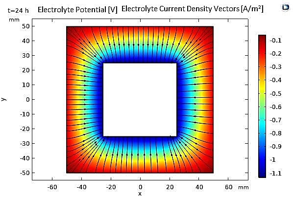
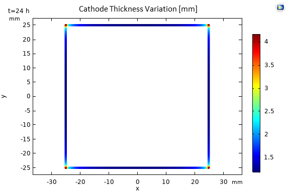
Figure 12 shows the thickness of the deposited layer after 24 hours (t=86400s) of deposition. We observe a uniform deposition of nickel on all sides of the cube, which is explained by the uniformity of the current density. However, the thickness variations at the corners are relatively significant, with a factor of 4 compared to the flat surfaces, which can be well explained by the tip effect.
On the other hand, Figure 13 allows for the analysis of the temporal evolution of the nickel deposition thickness on the cathodic boundaries, confirming the uniformity of the electroplated layer thickness, except at the cube cathode's corners. Additionally, the efficiency is calculated as the nickel deposition current density divided by the total current density at the cathode, which is approximately 97%, a value very close to what was previously found.
In another study, we attempted to develop a 3D electroplating model. We began by reproducing the same previous microstructure, consisting of cubic anode and cathode as shown in Figure 14. with the inter-electrode space filled with an electrolyte.
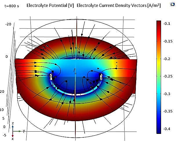
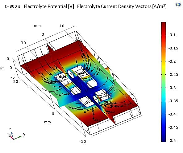
The numerical results of the 3D model, illustrated below, show that the electrolyte potential is higher near the anode and decreases towards the cathode, which is theoretically consistent. Additionally, the electrolyte current density vectors are clearly oriented from the anode to the cathode, as presented in Figure 15.
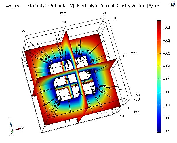
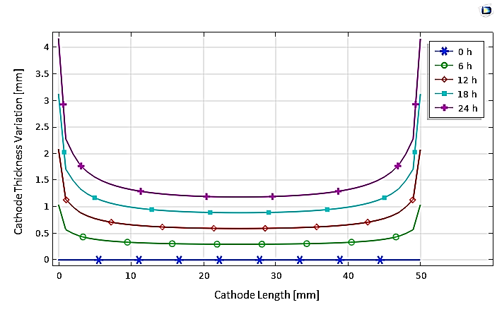
Furthermore, Figure 16 shows that the thickness of the electroplated layer after t=800s is uniform on the sides of the cathode, with a slight increase at the edges due to the edge effect, and at the corners due to the tip effect.
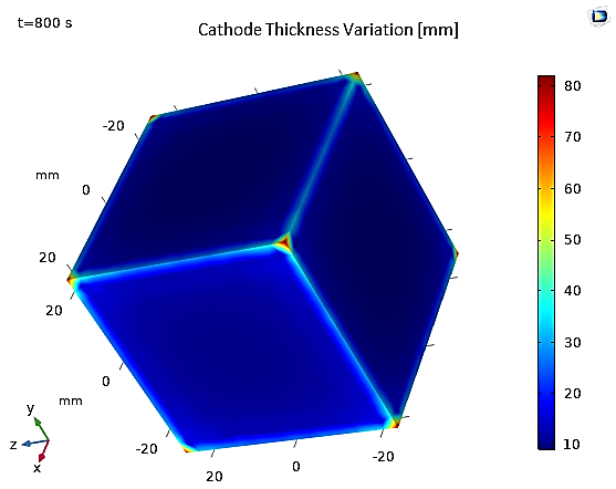
Table 3. Geometric Dimensions of the 3D Electroplating Structure of a Ring.
|
|
Shape |
Radius [mm] |
Height [mm] |
|
Cathode |
Inner Cylinder |
10 |
4 |
|
Outer Cylinder |
11 |
4 |
|
|
Anode |
Cylinder |
25 |
20 |
A comparison between the 2D and 3D electroplating models confirms that the results are qualitatively similar, although the maximum computation time differs, with the 3D model requiring significantly more computational time.
Another 3D application involves the electroplating of a small ring centered in an electrolyte, considered the cathodic electrode, surrounded by a cylindrical anode (see Figure 17). The dimensions of the model, including those of the cathode and anode, are presented in Table 3. The numerical results obtained for this application allow for the same observations regarding the potential and electrolyte current density vectors as in the previous study (see Figure 18).
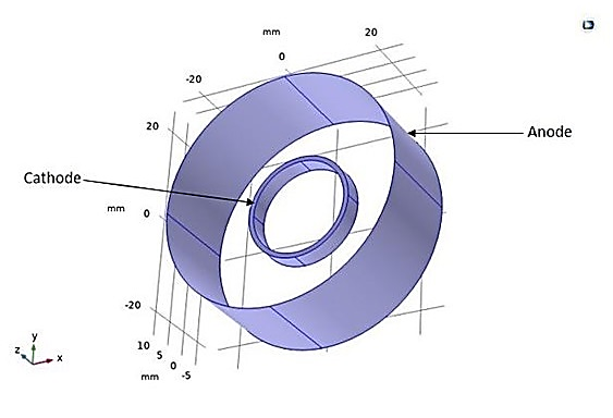
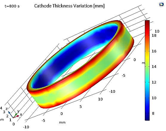
Figure 19 shows the thickness of the deposited layer after 800 seconds of deposition. Thickness variations are relatively significant, with more than a factor of 3 between the inner and outer parts of the ring. Additionally, the maximum deposition occurs at the edges of the ring. This suggests the need for improvements in the cell geometry to achieve a more uniform deposition thickness. Another alternative is to add active species on the surface, also known as leveling agents, which increase kinetic losses at the electrode surfaces. These leveling agents help maintain a uniform current density and, consequently, a more uniform deposit.
Another study involves the electroplating of a perforated rectangular piece (the cathode) immersed in an electrolyte solution, with a rectangular anode (see Figure 20). The dimensions of the model are presented in Table 4. As a result, the numerical results obtained after a deposition time of 800 seconds are illustrated by the figures below, showing the potential and electrolyte current density vectors (see Figure 21), as well as the deposition thickness on the cathodic piece, which is visibly non-uniform (see Figure 21).
Table 4. Geometric Dimensions of the 3D Electroplating Structure of a Perforated Piece.
|
|
Shape |
Width [mm] |
Depth [mm] |
|
Cathode |
Inner Block |
30 |
4 |
|
Outer Block |
50 |
14 |
|
|
Anode |
Block |
100 |
30 |
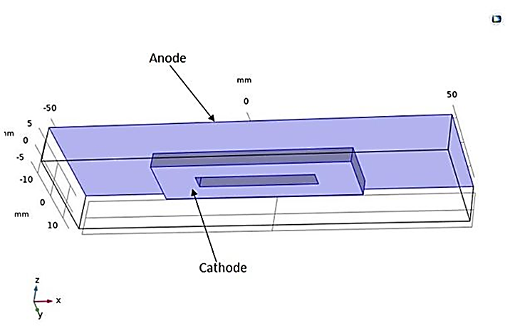
As shown in Figure 21 and Figure 22, this non-uniformity is explained by the shape of the anode, which does not allow for deposition on the lower face.
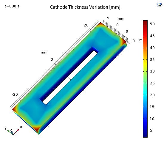 Figure 22. Total Variation in Cathode Thickness.
4. 3. Electropolishing
Another electroforming technology is Electropolishing which is a surface treatment that minimizes microroughness, enhances cleanability, and ensures polishing and passivation of surfaces. This can be achieved by switching the roles of the cathode and anode, with the anode being the piece undergoing electropolishing. This technique involves removing metal from a piece submerged in an electrolyte while passing an electric current through it. Generally, it is the reverse of electrodeposition: in electrodeposition, metal ions from the solution are deposited onto the piece, whereas in electropolishing, the piece is eroded and supplies metal ions to the electrolyte.
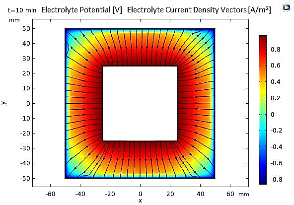
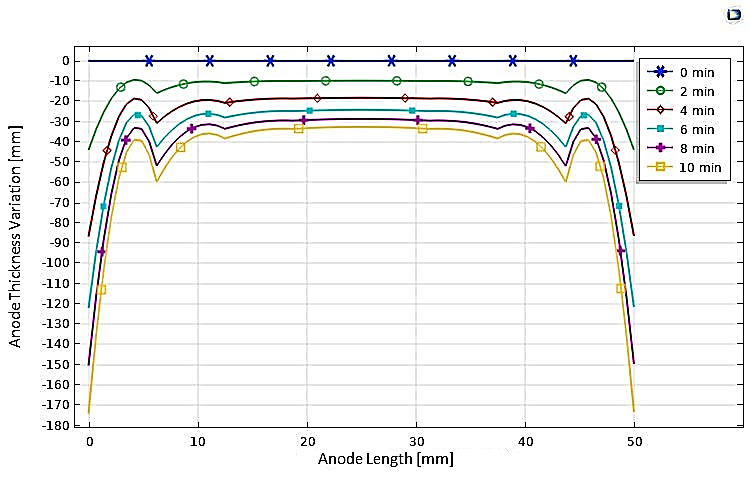
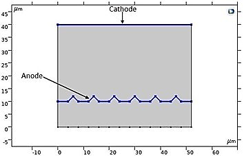
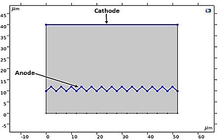
In our numerical investigation, we have simulated this technique. The potential and electrolyte current density are visualized in Figure 23, which shows a uniform distribution of potential from the cathode to the anode after a 10-minute (t=600s) electropolishing process. The variations in the thickness of the anode, illustrated in Figure 24, show near-uniform electropolishing on the sides of the anode, with significant emphasis at the vertices, which is entirely predictable. In order to highlight the significant effect of electropolishing, which allows for controlled surface leveling, we considered rough microstructure pieces with microscopically small and differently shaped teeth. The first piece had teeth with dimensions of 2 µm and spacings of 4 µm, while the second piece had more closely spaced teeth, with the same height of 2 µm. Both pieces (52 µm, 10 µm) are treated as positively charged anodes, facing negatively charged cathodes (see Figure 25 and Figure 26).
The numerical results of this electropolishing model allow us to track the temporal evolution of the surface treatment of anodic pieces and highlight the effects of this technique and its advantages in improving the appearance and performance of rough parts with defects, as shown in Figure 27 and Figure 28.
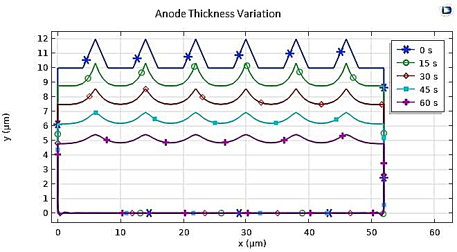
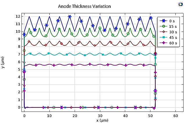
We can clearly observe the improvement in the surfaces and appearance of the pieces, even after a relatively short time of 1 min (t=60s). Through this application, we have highlighted the electropolishing process and its benefits in enhancing surfaces, providing them with anti-adhesive properties, particle resistance, or simply for brightness and aesthetic reasons.
4. 4. Discussion and Remarks
In this section, we discuss the key findings from our numerical evaluations of electroforming processes, specifically focusing on electroplating and electropolishing. This discussion includes comparisons with existing state-of-the-art research to provide a qualitative understanding of the effectiveness and accuracy of our models. Additionally, we explore the influence of key factors such as material properties, electrical parameters, and geometry on the uniformity and efficiency of the electroforming process.
By analyzing the thickness of the electroplated layer along cathodes with irregular shapes, it is clear that the deposition is always non-uniform, with significant accumulation at the edges of all the examined parts. However, comparison with the work of [21] can only be qualitative (see Table 5).
Table 5. Comparison of Thickness Distribution in Electroplating Models with State-of-the-art Works.
|
Characteristics |
Duration |
Thickness Distribution |
|
|
[21] |
Cathode of Irregular Shape |
/ |
1,74-16,45 µm |
|
Our Model |
2D Block |
24h (86400s) |
1,5-4 mm |
|
3D Block |
800s |
10–80 mm |
|
|
3D Ring |
800s |
8–20 mm |
|
|
Perforated Piece |
800s |
5–50 mm |
For what Concerns electropolishing, analyzing the temporal evolution of the process, i.e., the variation in the removed layer thickness over time, we can observe from Table 6 that there is an almost linear relationship, both in our numerical results and in the experimental works [22]. However, only a qualitative validation is possible due to differences in simulation parameters, especially the current value at the cathode.
Table 6. Comparison of Electropolished Layer Thickness Versus Time.
|
|
[22] |
Our Model |
|
|
Electropolishing Duration [s] |
0-300 |
0-600 |
|
|
Cathode Current Density [A/m2] |
/ |
500 |
|
|
The current of Electropolishing [A] |
0,3 |
0,6 |
/ |
|
Electropolished Layer Thickness d Vs t |
d=3,92e-4 t |
d=3,05e-4 t |
d=7,25e-3t (figure 24) |
Thus, 2D and 3D finite element models have been developed using COMSOL to analyze in detail the electroforming process with various applications: electrodeposition, electroplating, and electropolishing. Additionally, detailed parametric studies were conducted to address the effect of certain geometric and physical parameters on this process. The simulation results are theoretically predictable and consistent with previous findings (e.g., [23]-[25]). As conclusions that can be drawn from our assessment:
- Electroforming process is used for the construction and surface treatment of components of various shapes and sizes, particularly microstructures.
- Copper and nickel are the most commonly used materials in this process, offering significant advantages due to their behavior in conductive electrolytes. Nickel appears to be the most promising metal, as it provides higher and more uniform deposition.
- Electrical parameters, such as potential and current, strongly influence the deposition rate and its uniformity.
- The geometry of the electrodes and the electrolytic cell is a critical factor in this forming process, across all techniques.
- Another important parameter is the chemical composition of the electrolyte and, consequently, the ions involved in the electrochemical phenomenon responsible for electroforming.
5. Conclusions and Future Work
Electroforming is a promising technique that offers numerous possibilities for the fabrication of complex, high-quality components. Its potential continues to be explored and harnessed across various fields, positioning it to play a crucial role in future technological advancements and industrial innovation. The objective of this work was to numerically model the shaping of components, particularly surface treatment, using the electroforming process. The results obtained are theoretically validated and show good qualitative agreement with those found in subsequent studies.
In future work and as a continuation of this research, several improvements in the modeling of electroforming can be made, and certain limitations and assumptions can be eliminated. It would also be valuable to develop models with complex geometries to validate the capabilities of numerical models for simulating industrial applications. As well as investigating other emerging trends in Electroforming process (e.g., [26]-[30]).
References
[1] P. K. Rai, A. Gupta, "Electroforming Process for Microsystems Fabrication," Journal of The Electrochemical Society, vol. 170, no. 12, art. 123510, 2023. View Article
[2] A. M. Behagh, A. F. Tehrani, "Investigation and Modelling of Copper Electroforming Process for Surface Roughness Parameters using Regression and Pareto Anova Analyses," Surface Engineering and Applied Electrochemistry, vol. 59, no. 6, pp. 780-790, 2023. View Article
[3] H. J. Biswal, J. J. Kaur, P. R. Vundavilli, A. Gupta, "Recent Advances in Energy Field Assisted Hybrid Electrodeposition and Electroforming Processes," CIRP Journal of Manufacturing Science and Technology, vol. 38, pp. 518-546, 2022. View Article
[4] S. Syamsuir, F. B. Susetyo, B. Soegijono, S. D. Yudanto, B. Basori, M. K. Ajiriyanto, D. Edbert, E. U. M. Situmorang, D. Nanto, C. Rosyidan, "Rotating-magnetic-fieldassisted Electrodeposition of Copper for Ambulance Medical Equipment," Automotive Experiences, vol. 6, no. 2, pp. 290-302, 2023. View Article
[5] M. Jamesh, S. Kumar, T. Sankara Narayanan, "Electrodeposition of Hydroxyapatite Coating on Magnesium for Biomedical Applications," Journal of Coatings Technology and Research, vol. 9, pp. 495-502, 2012. View Article
[6] H. Bali, I. Hafsaoui, B. Makhlouf, "A Simultaneous Resolution Method for Coupling Field Circuit Equations for Steady-State Skin Effect Problems," in: Proceedings of 2018 IEEE International Conference on Electrical Sciences and Technologies in Maghreb, Algiers, Algeria, 2018, pp. 1-6. View Article
[7] I. Boutana, M. R. Mekideche, H. Bali, "Analysis Model and Numerical Investigation of Electromagnetic Tube Expansion with Field Concentrator," in: Proceedings of 20th IEEE International Multi-Conference on Systems, Signals & Devices, Mahdia, Tunisia, 2023, pp. 294-298. View Article
[8] I. Boutana, S. E. Bouferroum, A. Laouira, "Modeling of the Innovative Magnetic Pulse Joining Technology," in: Proceedings of 19th IEEE International Multi-Conference on Systems, Signals & Devices, Setif, Algeria, 2022, pp. 2115-2120. View Article
[9] I. Boutana, A. Bahloul, S. Boukendir, "Numerical Investigation on Weldability of Workpieces using Magnetic Pulse Welding Process," in: Proceedings of 2021 IEEE International Conference on Design & Test of Integrated Micro & Nano-Systems, Sfax, Tunisia, 2021, pp. 1-6.
[10] I. Boutana, M. E. Boussalem, A. Laouira, S. Bouferroum, "3D Modelling of the Mechanical Behaviour of Magnetic Forming Systems," Bulletin of Electrical Engineering and Informatics, vol. 11, no. 4, pp. 1807-1817, 2022. View Article
[11] I. Boutana, A. Bousba, Y. N. Benhadj, "Numerical Modeling of Industrial Parts Manufacturing using Electromagnetic Hemming Process," The International Journal of Advanced Manufacturing Technology, vol. 133, pp. 1943-1959, 2024. View Article
[12] I. Boutana, M. R. Mekideche, "Finite Element Model Analyzing Dynamical Behavior of Sheet Electromagnetic Forming," in: Proceedings of 6th IEEE International Multi-Conference on Systems, Signals and Devices, Djerba, Tunisia, 2009, pp. 1-6. View Article
[13] I. Boutana, O. Boultif, A. Zait, "Printed Circuit Boards Manufacturing using Electrodeposition Process: An Innovative Numerical Model," in Proceedings of 10th World Congress on Electrical Engineering and Computer Systems and Sciences, Barcelona, Spain, 2024, art. 103. View Article
[14] E. Andreou, S. Roy, "Modelling and Verification of the Nickel Electroforming Process of a Mechanical Vane Fit for Industry 4.0," Digital Chemical Engineering, art. 100177, 2024. View Article
[15] Y. Li, X. Wei, H. Liu, Y. Sun, "Flotation Assisted Electrodeposition Process to Recover Copper From Waste Printed Circuit Boards," Chemical Engineering Journal, art. 154747, 2024. View Article
[16] M. R. Akbarpour, M. Fathi, F. Gharibi Asl, H. S. Kim, "Effects of Carbon Allotrope Type on Microstructural and Electrochemical Properties of Ni-C Nanocomposite Coating Prepared by Pulse-Reverse Electrodeposition Method," Metals and Materials International, pp. 1-11, 2024. View Article
[17] T. Chen, Q. Huang, H. Zhu, Y. Ma, "The Characterisation of Passivation and Colouring of Zn-Ni Electroplated 2024 Aluminium Alloy in the Presence of Cu+," Transactions of the IMF, pp. 1-6, 2024. View Article
[18] D. Colombo, L. Carro, C. Catellani, S. Ceré, "Electropolishing of AISI 316L: Effect on Surface Characteristics and Corrosion Behavior," The International Journal of Advanced Manufacturing Technology, vol. 130, no. 9, pp. 4207-4219, 2024. View Article
[19] R. Maexa, "Nernst-Planck Equation," in: Encyclopedia of Computational Neuroscience, Springer, 2022, pp. 2182-2187. View Article
[20] E. J. Dickinson, A. J Wain, "The Butler-Volmer Equation in Electrochemical Theory: Origins, Value, and Practical Application," Journal of Electroanalytical Chemistry, vol. 872, art. 114145, 2020. View Article
[21] W. Giurlani, G. Pappaianni, F. Biffoli, E. Mariani, M. Bonechi, L. Giliberti, M. Tufarelli, P. Franzo, E. Cianfanelli, M. Innocenti, "What Is the Current State of Sustainability in the Decorative Electroplating Industry? A Close Look at New Practices and Advances," Sustainability, vol. 16, pp. 1-31, 2024. View Article
[22] E. Gadalińska, W. W. Wojciech, "Electropolishing Procedure Dedicated to In-Depth Stress Measurements with X-ray Diffractometry," Fatigue of Aircraft Structures, vol. 2016, no. 8, pp. 65-72, 2016. View Article
[23] Q. Q. Zhu, H. Y. Li, Y. Wang, "Low Current Density Electropolishing and Corrosion Resistance Study of 304 Stainless Steel," Surface Engineering, vol. 40, no 1, pp. 25-33, 2024. View Article
[24] C. Hu, L. Tang, X. Zhang, "A Rapid One-Step Electrodeposition Method for Fabrication of the Superhydrophobic Nickel/Cobalt Alloy Surfaces with Excellent Robustness and Durability Features," Surfaces and Interfaces, vol. 44, art. 103824, 2024. View Article
[25] L. Shuai, Da, Min, A. Imran, "Recovery of Nickel from Actual Electroplating wastewater by Integrated Electrodeposition with Adsorption Pretreatment Technique," Process Safety and Environmental Protection, vol. 172, pp. 417-424, 2023. View Article
[26] Y. Wang, H. Wang, X. Chen, Y. Shang, H. Wang, Z. An, J. Zheng, S. Wang, "Self-Learning Effect of Csfamapbibr Memristor Achieved by Electroforming Process," Materials Chemistry and Physics, vol. 310, art. 128488, 2023. View Article
[27] S. Son, C. L. Torre, A. Kindsmuller, V. Rana, S. Menzel, "A Study of the Electroforming Process in 1t1r Memory Arrays," IEEE Transactions on Computer-Aided Design of Integrated Circuits and Systems, vol. 42, no. 2, pp. 558-568, 2023. View Article
[28] H. Wang, J. Xing, T. Fan, J. Liu, J. Xie, C. Li, "An Effect of Layered Auxiliary Cathode on Thickness Uniformity in Micro Electroforming Process," Micromachines, vol. 14, no. 7, art. 1307, 2023. View Article
[29] J. Setiawan, A. Sudiarso, I. Winursitoc, M. Herliansyah, "Influence of Concentration of Copper Electrolyte, Voltage, and Time of Electroforming on Conductive Acrylonitrile Butadiene Styrene Parts on Deposition Rate and Microstructure," International Journal of Engineering, vol. 37, no. 10, pp. 1914-1925, 2024. View Article
[30] Y. Zhang, P. Ming, X. Zhang, X. Li, L. Li, Z. Yang, "Jet Electroforming of High-Aspectratio Microcomponents" by Periodically Lifting a Necked-Entrance through-mask," Micromachines, vol. 15, no. 6, art. 753, 2024. View Article